A glass is a typical insulator, but it easily turns into an excellent conductor by coating the glass with a transparent conductive oxide (TCO) film. TCO film is an essential material in opt electronic devices, such as a ceramic heater, anti-static shield glass, touch panel, and liquid-crystal monitor, and the industrial film formation technique should be developed to meet these demands.
Our research group developed a spray pyrolysis deposition (SPD) technique to prepare TCO film by a joint research project with MAKE Co. Ltd., and SPD Laboratory Co. Ltd., in Hamamatsu, Japan. SPD is the same film processing technique as so-called pyrosol technique, in which a source solution is sprayed on the heated substrate to be pyrolized and deposited as a film. High-frequency plasma and electromagnetic wave have also been employed as a new energy source for a novel film formation technique. These film formation techniques are applied to fabricate opt electronic devices, such as dye-sensitized solar cell and UV sensor, as well as TCO films.
Research topics
TCO film on a large (30cm×30cm) substrate
The substrate from the size of 2cm×2cm to 30cm×30cm is acceptable to deposit TCO film by SPD technique. FTO film with high transmittance, >80% in the visible region, and low electrical resistivity, 1×10⁻⁴ Ω⋅cm, is prepared in air within 10 minutes in a laboratory scale.
Novel TCO film
Novel TCO films, such as TNO, IZO and AZO, along with the conventional ones, ITO and FTO, are prepared and applied to opt electric devices mentioned below.
Dye-sensitized solar cell
The optical and electrical properties of TCO films are optimized and applied to dye-sensitized solar cells to achieve high light-to-electron conversion efficiency. Porous TiO2 layer is deposited on the TCO film by SPD technique to prepare a working electrode for a dye-sensitized solar cell.
Magnetic and dielectric material for devices
TCO is not the only material that is prepared by SPD technique. The technique is also applicable to deposit ferrite and barium titanate films.
Optical sensor
UV sensor with p-i-n junction by stacking metal oxide layers is fabricated by SPD technique. The sensitivity is easily tuned by controlling the surface morphology and/or the carrier density of i-layer.
High-frequency plasma and electromagnetic wave
The interaction between precursors and plasma or electromagnetic wave induces a new chemical reaction to prepare TCO film. Additionally, plasma induced by a surface discharge can supply a high energy to the selective area on the substrate, which is a convenient tool for a direct patterning in a film formation.
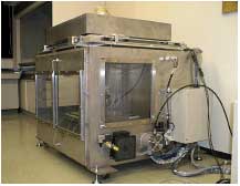
Apparatus of spray pyrolysis deposition (SPD) technique. A large substrate up to 30 × 30 cm in size is acceptable in this system. A compact SPD film formation system for a laboratory scale was also developed.
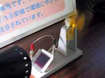
Demonstration of a dye-sensitized solar cell in Techno-Festa in Hamamatsu. An electric motor is working by a single cell under the quasi-sunlight irradiation.
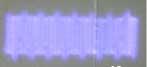
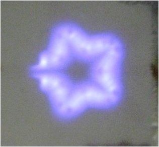
Surface discharge on the selec-tive area for a direct patterning in film formation; (top) Plane, (left) Star, and (right) Symbol of Shizuoka University; Suruga Bay with Mt. Fuji, where was selected as a World Heritage site in UNESCO, 2013.